Welcome To Dellux!
Welcome To Dellux!
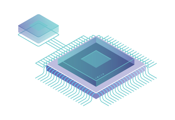
VLSI design stands for “Very Large Scale Integration”, it is used to create IC (Integrated Circuits) by combining millions of metal oxide silicon (MOS) transistors to form a single chip. VLSI came into existence in the 1970s.
VLSI design has been widely used in various devices such as memory cards, cell phones, and set-top boxes, which perform various roles by allowing the use of billions of transistors in a single chip. VLSI is a revolutionary invention in the field of electronics, it gives freedom to the designers to create devices without worrying about the size, and cost of production.
VLSI design is a Post-Graduate course in technology that offers various programs such as –M.Tech In VLSI Design And Technology, M.Tech In VLSI Design, PG Diploma In VLSI Design, PG Certificate In VLSI Design, M.E. in VLSI Design, M.Sc. in VLSI Design And Technology.
Overall, VLSI IC design incorporates two primary stages or parts: